It’s no secret that artificial intelligence (AI) is driving innovation, particularly when it comes to processing data at scale. Machine learning (ML) and deep learning (DL) algorithms, designed to solve complex problems and self-learn over time, are exploding the possibilities of what computers are capable of.
As the problems we ask computers to solve get more complex, there’s also an unavoidable, explosive growth in the number of processes they run. This growth has led to the rise of specialized processors and a whole host of new acronyms.
Joining the ranks of central processing units (CPUs), which you may already be familiar with, are neural processing units (NPUs), graphics processing units (GPUs), and tensile processing units (TPUs).
So, let’s dig in to understand how some of these specialized processors work, and how they’re different from each other. If you’re still with me after that, stick around for an IT history lesson. I’ll get into some of the more technical concepts about the combination of hardware and software developments in the last 100 or so years.
Central Processing Unit (CPU): The OG
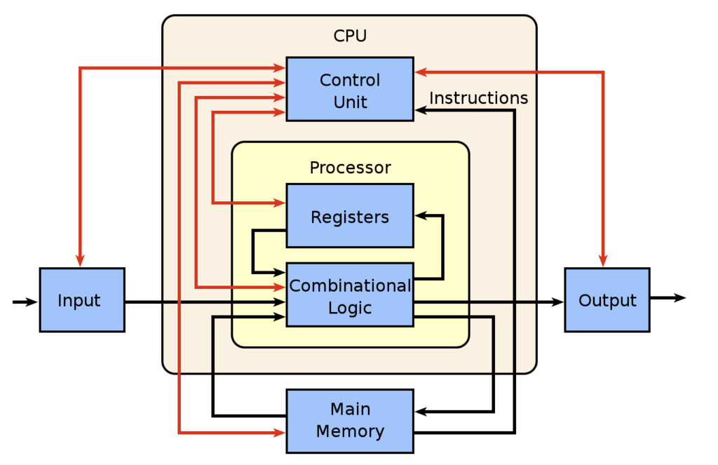
Think of the CPU as the general of your computer. There are two main parts of a CPU, an arithmetic-logic unit (ALU) and a control unit. An ALU allows arithmetic (add, subtract, etc.) and logic (AND, OR, NOT, etc.) operations to be carried out. The control unit controls the ALU, memory, and input/output (IO) functions, which tells them how to respond to the program that’s just been read from the memory.
The best way to track what the CPU does is to think of it as an input/output flow. The CPU will take the request (input), access the memory of the computer for instructions on how to perform that task, delegate the execution to either its own ALUs or another specialized processor, take all that data back into its control unit, then take a single, unified action (output).
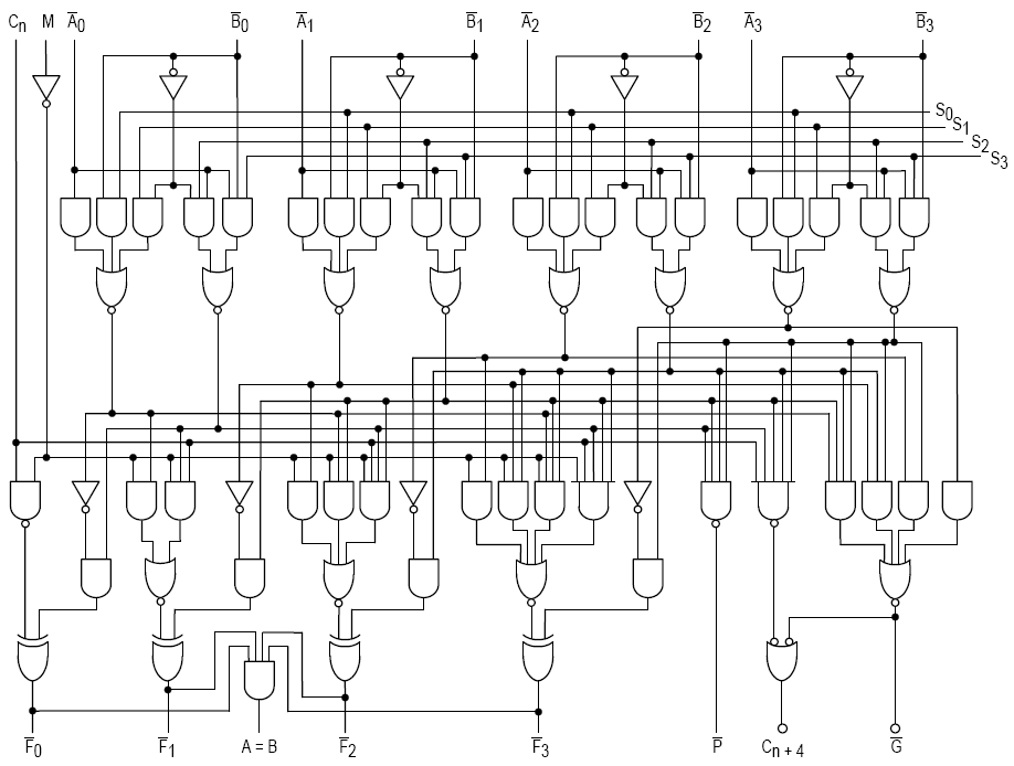
For a visual, this is the the circuitry map for an ALU from 1970:
But, more importantly, here’s a logic map about what a CPU does:
CPUs have gotten more powerful over the years as we’ve moved from single-core processors to multicore processors. Basically, there are several ALUs executing tasks that are being managed by the CPU’s control unit, and they perform tasks in parallel. That means that it works well in combination with specialized AI processors like GPUs.
The Rise of Specialized Processors
When a computer is given a task, the first thing the processor has to do is communicate with the memory, including program memory (ROM)—designed for more fixed tasks like startup—and data memory (RAM)—designed for things that change more often like loading applications, editing a document, and browsing the internet. The thing that allows these elements to talk is called the bus, and it can only access one of the two types of memory at one time.
In the past, processors ran more slowly than memory access, but that’s changed as processors have gotten more sophisticated. Now, when CPUs are asked to do a bunch of processes on large amounts of data, the CPU ends up waiting for memory access because of traffic on the bus. In addition to slower processing, it also uses a ton of energy. Folks in computing call this the Von Neumann bottleneck, and as compute tasks like those for AI have become more complex, we’ve had to work out ways to solve this problem.
One option is to create chips that are optimized to specific tasks. Specialized chips are designed to solve the processing difficulties machine learning algorithms present to CPUs. In the race to create the best AI processor, big players like Google, IBM, Microsoft, and Nvidia have solved this with specialized processors that can execute more logical queries (and thus more complex logic). They achieve this in a few different ways. So, let’s talk about what that looks like: What are GPUs, TPUs, and NPUs?
Graphics Processing Unit (GPU)
GPUs started out as specialized graphics processors and are often conflated with graphics cards (which have a bit more hardware to them). GPUs were designed to support massive amounts of parallel processing, and they work in tandem with CPUs, either fully integrated on the main motherboard, or, for heavier loads, on their own dedicated piece of hardware. They also use a ton of energy and thus generate heat.
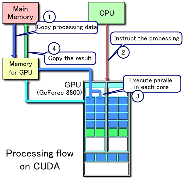
GPUs have long been used in gaming, and it wasn’t until the 2000s that folks started using them for general computing—thanks to Nvidia. Nvidia certainly designs chips, of course, but they also introduced a proprietary platform called CUDA that allows programmers to have direct access to a GPU’s virtual instruction set and parallel computational elements. This means that you can set up compute kernels, or clusters of processors that work together and are ideally suited to specific tasks, without taxing the rest of your resources. Here’s a great diagram that shows the workflow:
This made GPUs wildly applicable for machine learning tasks, and they benefited from the fact that they leveraged existing, well-known processes. What we mean by that is: oftentimes when you’re researching solutions, the solution that wins is not always the “best” one based on pure execution. If you’re introducing something that has to (for example) fundamentally change consumer behavior, or that requires everyone to relearn a skill, you’re going to have resistance to adoption. So, GPUs playing nice with existing systems, programming languages, etc. aided wide adoption. They’re not quite plug-and-play, but you get the gist.
As time has gone on, there are now also open source platforms that support GPUs that are supported by heavy-hitting industry players (including Nvidia). The largest of these is OpenCL. And, folks have added tensor cores, which this article does a fabulous job of explaining.
Tensor Processing Unit (TPU)
Great news: the TL:DR of this acronym boils down to: It’s Google’s proprietary AI processor. They started using them in their own data centers in 2015, released them to the public in 2016, and there are some commercially available models. They run on ASICs (hard-etched chips I’ll talk more about later) and Google’s TensorFlow software.
Compared with GPUs, they’re specifically designed to have slightly lower precision, which makes sense given that this makes them more flexible to different types of workloads. I think Google themselves sum it up best:
If it’s raining outside, you probably don’t need to know exactly how many droplets of water are falling per second—you just wonder whether it’s raining lightly or heavily. Similarly, neural network predictions often don’t require the precision of floating point calculations with 32-bit or even 16-bit numbers. With some effort, you may be able to use 8-bit integers to calculate a neural network prediction and still maintain the appropriate level of accuracy.
Google Cloud Blog
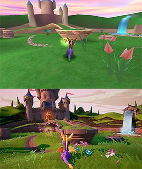
GPUs, on the other hand, were originally designed for graphics processing and rendering, which relies on each point’s relationship to each other to create a readable image—if you have less accuracy in those points, you amplify that in their vectors, and then you end up with Playstation 2 Spyro instead of Playstation 4 Spyro.
Another important design choice that deviates from CPUs and GPUs is that TPUs are designed around a systolic array. Systolic arrays create a network of processors that are each computing a partial task, then sending it along to the next node until you reach the end of the line. Each node is usually fixed and identical, but the program that runs between them is programmable. It’s called a data processing unit (DPU).
Neural Processing Unit (NPU)
“NPU” is sometimes used as the category name for all specialized AI processors, but it’s more often specifically applied to those designed for mobile devices. Just for confusion’s sake, note that Samsung also refers to its proprietary chipsets as NPU.
NPUs contain all the necessary information to complete AI processing, and they run on a principle of synaptic weight. Synaptic weight is a term adapted from biology which describes the strength of connection between two neurons. Simply put, in our bodies if two neurons find themselves sharing information more often, the connection between them becomes literally stronger, making it easier for energy to pass between them. At the end of the day, that makes it easier for you to do something. (Wow, the science between habit forming makes a lot more sense now.) Many neural networks mimic this.
When we say AI algorithms learn, this is one of the ways—they track likely possibilities over time, and give more weight to that connected node. The impact is huge when it comes to power consumption. Parallel processing runs each task next to each other, but isn’t great at accounting for the completion of tasks, especially as your architecture scales and processing units might be more separate.
Quick Refresh: Neural Networks and Decision Making in Computers
As we discuss in AI 101, when you’re thinking about the process of making a decision, what you see is that you’re actually making many decisions in a series, and often the things you’re considering before you reach your final decision affect the eventual outcome. Since computers are designed on a strict binary, they’re not “naturally” suited to contextualizing information in order to make better decisions. Neural networks are the solution. They’re based on matrix math, and they look like this:
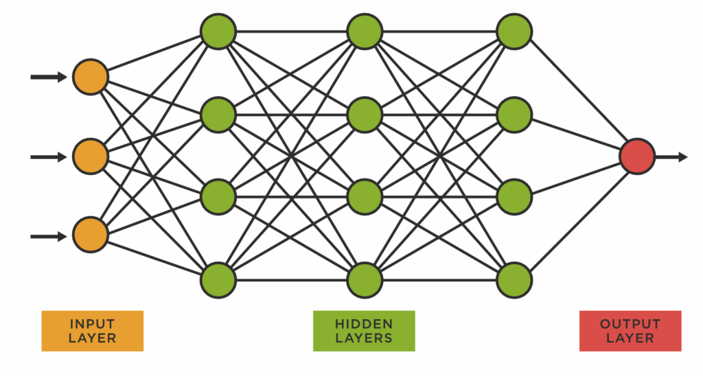
Basically, you’re asking a computer to have each potential decision check in with all the other possibilities, to weigh the outcome, and to learn from their own experience and sensory information. That all translates to more calculations being run at one time.
Recapping the Key Differences
That was a lot. Here’s a summary:
- Functionality: GPUs were developed for graphics rendering, while TPUs and NPUs are purpose-built for AI/ML workloads.
- Parallelism: GPUs are made for parallel processing, ideal for training complex neural networks. TPUs take this specialization further, focusing on tensor operations to achieve higher speeds and energy efficiencies.
- Customization: TPUs and NPUs are more specialized and customized for AI tasks, while GPUs offer a more general-purpose approach suitable for various compute workloads.
- Use Cases: GPUs are commonly used in data centers and workstations for AI research and training. TPUs are extensively utilized in Google’s cloud infrastructure, and NPUs are prevalent in AI-enabled devices like smartphones and Internet of Things (IoT) gadgets.
- Availability: GPUs are widely available from various manufacturers and accessible to researchers, developers, and hobbyists. TPUs are exclusive to Google Cloud services, and NPUs are integrated into specific devices.
Do the Differences Matter?
The definitions of the different processors start to sound pretty similar after a while. A multicore processor combines multiple ALUs under a central control unit. A GPU combines more ALUs under a specialized processor. A TPU combines multiple compute nodes under a DPU, which is analogous to a CPU.
At the end of the day, there’s some nuance about the different design choices between processors, but their impact is truly seen at scale versus at the consumer level. Specialized processors can handle larger datasets more efficiently, which translates to faster processing using less electrical power (though our net power usage may go up as we use AI tools more).
It’s also important to note that these are new and changing terms in a new and changing landscape. Google’s TPU was announced in 2015, just eight years ago. I can’t count the amount of conversations I’ve had that end in a hyperbolic impression of what AI is going to do for/to the world, and that’s largely because people think that there’s no limit to what it is.
But, the innovations that make AI possible were created by real people. (Though, maybe AIs will start coding themselves, who knows.) And, chips that power AI are real things—a piece of silicon that comes from the ground and is processed in a lab. Wrapping our heads around what those physical realities are, what challenges we had to overcome, and how they were solved, can help us understand how we can use these tools more effectively—and do more cool stuff in the future.
Bonus Content: A Bit of a History of the Hardware
Which brings me to our history lesson. In order to more deeply understand our topic today, you have to know a little bit about how computers are physically built. The most fundamental language of computers is binary code, represented as a series of 0s and 1s. Those values correspond to whether a circuit is closed or open, respectively. When a circuit is closed, you cannot push power through it. When it’s open, you can. Transistors regulate current flow, generate electrical signals, and act as a switch or gate. You can connect lots of transistors with circuitry to create an integrated circuit chip.
The combination of open and closed patterns of transistors can be read by your computer. As you add more transistors, you’re able to express more and more numbers in binary code. You can see how this influences the basic foundations of computing in how we measure bits and bytes. Eight transistors store one byte of data: two possibilities for each of the eight transistors, and then every possible combination of those possibilities (2^8) = 256 possible combinations of open/closed gates (bits), so 8 bits = one byte, which can represent any number between 0 and 255.
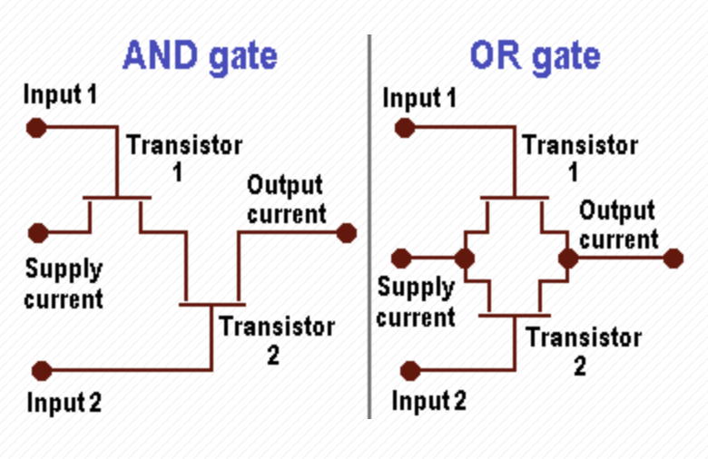
Improvements in reducing transistor size and increasing transistor density on a single chip has led to improvements in capacity, speed, and power consumption, largely due to our ability to purify semiconductor materials, leverage more sophisticated tools like chemical etching, and improve clean room technology. That all started with the integrated circuit chip.
Integrated circuit chips were invented around 1958, fueled by the discoveries of a few different people who solved different challenges nearly simultaneously. Jack Kilby of Texas Instruments created a hybrid integrated circuit measuring about 7/16” by 1/16” (11.1 mm by 1.6 mm). Robert Noyce (eventual co-founder of Intel) went on to create the first monolithic integrated circuit chip (so, all circuits held on the same chip) and it was around the same size. Here’s a blown-up version of it, held by Noyce:

Note those first chips only held about 60 transistors. Current chips can have billions of transistors etched onto the same microchip, and are even smaller. Here’s an example of what a integrated circuit looks like when it’s exposed:
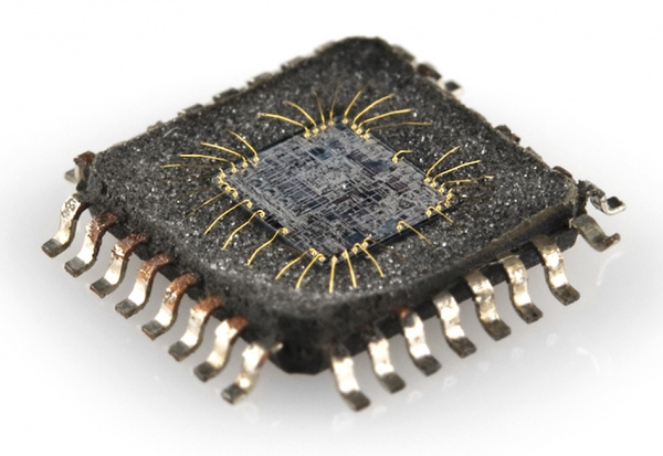
And, for reference, that’s about this big:

And, that, folks, is one of the reasons you can now have a whole computer in your pocket in the guise of a smartphone. As you can imagine, something the size of a modern laptop or rack-mounted server can combine more of these elements more effectively. Hence, the rise of AI.
One More Acronym: What are FPGAs?
So far, I’ve described fixed, physical points on a chip, but chip performance is also affected by software. Software represents the logic and instructions for how all these things work together. So, when you create a chip, you have two options: you either know what software you’re going to run and create a customized chip that supports that, or you get a chip that acts like a blank slate and can be reprogrammed based on what you need.
The first method is called application-specific integrated circuits (ASIC). However, just like any proprietary build in manufacturing, you need to build them at scale for them to be profitable, and they’re slower to produce. Both CPUs and GPUs typically run on hard-etched chips like this.
Reprogrammable chips are known as field-programmable gate arrays (FPGA). They’re flexible and come with a variety of standard interfaces for developers. That means they’re incredibly valuable for AI applications, and particularly deep learning algorithms—as things rapidly advance, FPGAs can be continuously reprogrammed with multiple functions on the same chip, which lets developers test, iterate, and deliver them to market quickly. This flexibility is most notable in that you can also reprogram things like the input/output (IO) interface, so you can reduce latency and overcome bottlenecks. For that reason, folks will often compare the efficacy of the whole class of ASIC-based processors (CPUs, GPUs, NPUs, TPUs) to FPGAs, which, of course, has also led to hybrid solutions.
Summing It All Up: Chip Technology is Rad
Improvements in materials science and microchip construction laid the foundation for providing the processing capacity required by AI, and big players in the industry (Nvidia, Intel, Google, Microsoft, etc.) have leveraged those chips to create specialized processors.
Simultaneously, software has allowed many processing cores to be networked in order to control and distribute processing loads for increased speeds. All that has led us to the rise in specialized chips that enable the massive demands of AI.
Hopefully you have a better understanding of the different chipsets out there, how they work, and the difference between them. Still have questions? Let us know in the comments.


